
Do you know the meaning of each layer of PCB
PCB, namely printed circuit board, is one of the important parts of electronic industry bar. Almost every kind of electronic equipment, from electronic watches and calculators to computers, communication electronic equipment and military weapon systems, as long as there are electronic components such as integrated circuits, printed boards are used to electrically interconnect the components. Printed circuit board (PCB) is composed of insulating bottom plate, connecting wires and pads for assembling and welding electronic components, which has the dual functions of conducting lines and insulating bottom plate. It can replace complex wiring and realize the electrical connection between components in the circuit, which not only simplifies the assembly and welding of electronic products. Below, Shenzhen Lianxiaobian will take you to understand the meaning of each layer of PCB.We have every reason to believe. china aluminum pcb assembly factory It will become the mainstream of the industry and will gradually affect more and more people. https://intechcircuit.com/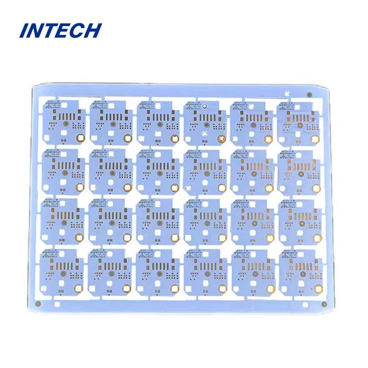
There are many layers used in PCB design in PCB factory: mechanical layer, keepout layer forbidden wiring layer, Signal layer signal layer, Internal plane layer internal power/grounding layer, top overlay screen printing layer, bottom overlay screen printing layer, Top paste top flux layer, bottom paste bottom flux layer, top solder top solder resist layer, bottom solder bottom solder resist layer, drill guide via guide layer, drill drawing via drilling layer, and multilayer.
Top signal layer (Top Layer):
Also known as component layer, it is mainly used for placing components, and can be used for wiring for double-layer boards and multi-layer boards.
Intermediate signal layer (Mid Layer):
There can be up to 30 layers, which are used for laying signal lines in multilayer boards.
Bottom signal layer:
Also known as welding layer, it is mainly used for wiring and welding, and sometimes components can be placed.
Top overlay:
It is used to mark the projection outline of components, the label, nominal value or model of components and various annotation characters.
Bottom overlay:
Same as the top screen printing layer, if all kinds of labels are included in the top screen printing layer, then the bottom screen printing layer is unnecessary.
Internal Plane plane:
It is usually called the inner electrical layer, including the power supply layer, the reference power supply layer and the ground plane signal layer. The internal power layer is output in the form of negative film.
Mechanical Layer (mechanical layer):
The mechanical layer defines the appearance of the whole PCB, and it is generally used to set the external dimensions, data marks, alignment marks, assembly instructions and other mechanical information of the circuit board.
Altium Designer provides 16 mechanical layers, which are generally used to set the overall dimensions, data marks, alignment marks, assembly instructions and other mechanical information of the circuit board. This information varies according to the requirements of design companies or PCB manufacturers. In addition, the mechanical layer can be attached to other layers to output the display together.
Solder mask (solder mask):
Altium Designer provides two solder resist layers: Top Solder (top layer) and Bottom Solder (bottom layer).
There are two layers of Top solder Mask and Bottom Solder Mask, which are automatically generated by Protel PCB corresponding to the data of pads and vias in circuit board files, and are mainly used for laying solder resist paint. This board adopts negative output, so the pads and vias displayed on the board represent the areas on the circuit board that are not covered with solder resist paint, that is, the parts that can be soldered.
Because it is a negative output, in fact, the actual effect of the part with Solder Mask is not green oil, but tin plating, which is silvery white! Apply a layer of paint, such as solder mask, to all parts other than the pad to prevent these parts from being tinned. Solder resist is used to match pads in the design process and is automatically generated.
Solder mask is the solder mask, which refers to the part of the board to be painted with green oil. In fact, this solder mask uses negative output, so after the shape of the solder mask is mapped to the board, it is not the green oil solder mask, but the copper skin is exposed. Usually, in order to increase the thickness of copper skin, the solder mask is crossed to remove green oil, and then tin is added to increase the thickness of copper wire.
Apply a layer of paint to all parts outside the pad. We usually use green oil and blue oil to prevent these parts from being tinned. Solder resist is used to match pads in the design process and is automatically generated. The solder mask is a negative output, the solder mask is not covered with oil, and the other parts are covered with oil.